SNES Controller PCB Instructions
Posted on Sat 15 April 2023 in Instructions
1. Preparation
Note
I put some Amazon Affiliate links in this section. I get a miniscule commission (at no cost to you) if you buy stuff with these links, but every little bit helps right?
Required Tools
You need some basic soldering equipment for this:
- Soldering Iron and Solder (I use this one)
- De-Soldering Braid (to clean up solder bridges - accidental or intentional)
- Flux (like this stuff)
- Tweezers
Optional Tools
These tools are mostly only needed if you're going to replace the connector on the end of the SNES controller cable that plugs into the PCB.
- Wire cutting tool
- Wire stripping tool
- Dupont terminal crimping tool (like this one)
Donor Components
If you are repairing a broken controller, you should harvest the following components from the original unit:
- Shell, screws, d-pad, buttons, shoulder button pivot pins, and membranes.
- Alternative: Transparent d-pad, buttons, and membranes to take advantage of the optional LEDs.
- Shoulder button daughter boards and wires.
- Alternative: Fabricate new shoulder button daughter boards.
- Wire-to-board header that mates with the original connector on the controller cable.
- Alternative: Use a Molex Mini-SPOX™ connector as documented in Wire-to-Board Header/Option 2
Required Knowledge
I'm not going to try and teach you any of these things in these instructions, so best come prepared. You should already know:
- How to use all of the tools on the Required and Optional lists.
- How to solder and de-solder through-hole and surface-mount components.
- How to handle static-sensitive parts.
- Basic electronic safety precautions.
Before You Begin
- Carefully sort and identify your parts. Some of the components used in this project can be easily confused with each other, notably the CD4021B shift register and CD4011B quad-NAND gate ICs.
- Make sure you understand how to identify proper polarity for all components. Refer to the manufacturer datasheet if you have any doubts.
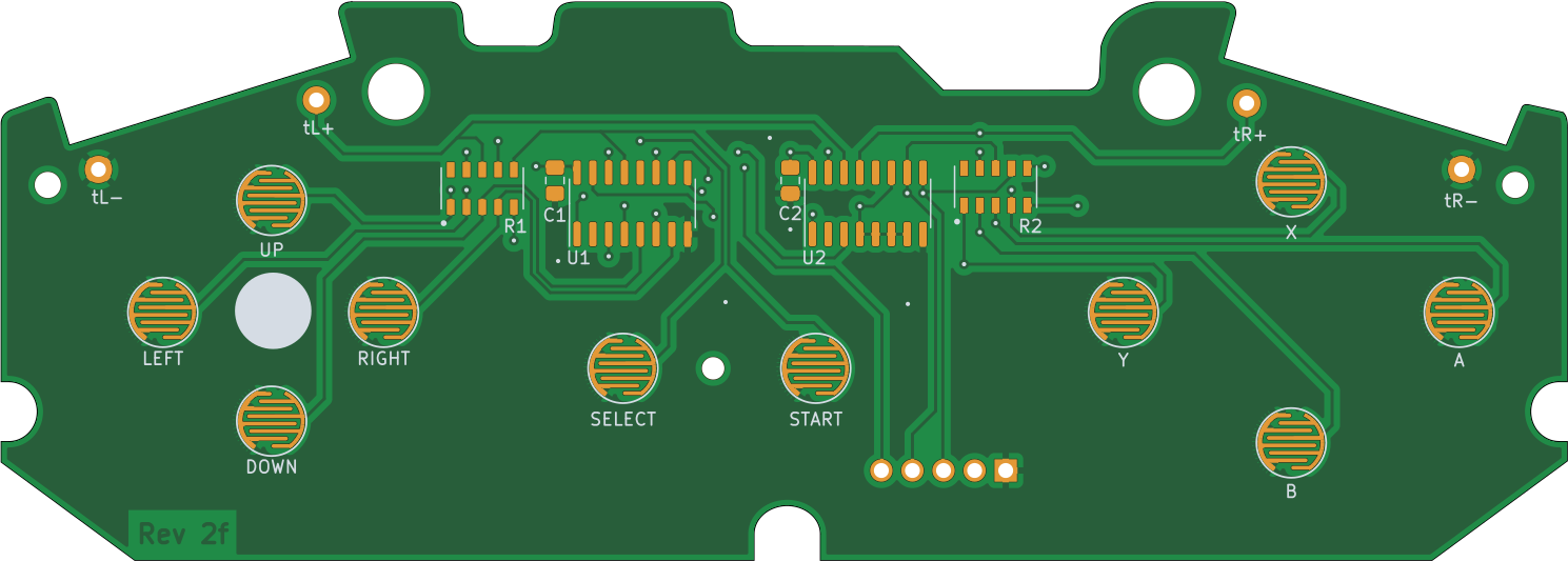
- Take a minute to familiarize yourself with the PCB layout and conventions used in the silkscreen markings:
- Where applicable, PIN 1 is identified with a (white dot) and longer line.
- The negative/cathode end of LEDs are marked with a line.
- The proper orientation of the wire-to-board header is indicated with a line around the outside and, in the case of the Nintendo OEM footprint, keyed with peg holes.
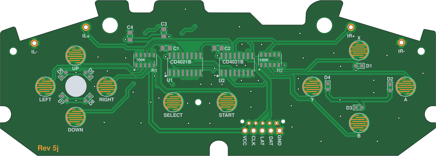
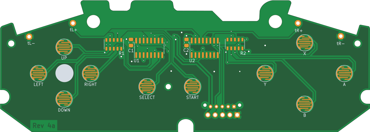
Documented Board Revisions
I've released multiple PCB revisions over the course of this project, and this document attempts to apply to all of them by informing you which board revisions each section applies to.
I would hope you are using the most recent revision available, but I know I have a handful of older prototypes laying around, and I'm probably not the only one. I've marked the board revision on the front of each PCB release, but you may also find these images helpful to identify your particular board revision.


Attention
If you still have some of these, hey I get it: these things cost money! Even so, fore your sanity's sake I recommend that you throw them out and replace them with a newer revision. Sadly, the rev_2f revision had a design flaw that required a bodged-in fix to work with all games.
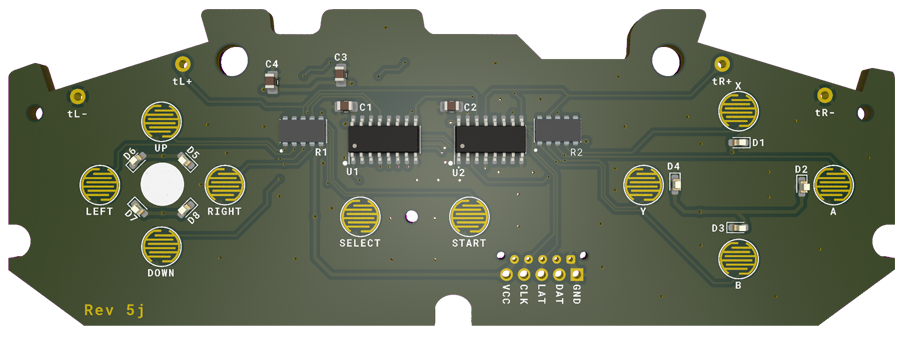
2. Basic Controller Function
Applicable Board Revisions: ALL
This section populates the components required for this SNES controller PCB to be a SNES controller.
Required BoM Components
| Ref | Mfg. Part # | Quantity | Description |
|---|---|---|---|
| U1, U2 | CD4021B |
2 | CMOS 8-Stage Static Shift Register |
| R1, R2 | 745C101104JP |
2 | Resistor array, 100Kohms 50V 5% |
| C1, C2 | 885012007076 |
2 | Multilayer Ceramic Capacitors MLCC - SMD/SMT WCAP-CSGP 100V 10pF 0805 5% |
Assembly Steps - Part 1
Applicable Board Revisions: ALL
- Solder 10pF SMD capacitors at C1 and C2.
- Solder 100K resistor arrays at R1 and R2. Pin 1 is marked by a dot, but it doesn't really matter for this particular type of resistor array.
- Solder CD4021B shift registers at U1 and U2. Pin 1 is marked by a , and in this case it very much does matter.
Note
If you're using a rev_4 or older PCB that doesn't have footprints for LEDs or the SOCD filter circuit, go ahead and skip to section 5. Wire-to-Board Header.
3. OPTIONAL Lighted Buttons
Applicable Board Revisions: rev_5j and newer
These steps are only required if you want your controller buttons and d-pad to light up. And really, who doesn't?
Required BoM Components
| Ref | Mfg. Part # | Quantity | Description |
|---|---|---|---|
| D1, D2, D3, D4, D5, D6, D7, D8 | LSM0603443V |
8 | Standard LED, SMD 0603 3V 330mcd WHITE |
| R3, R4 | 0805W8J0101T5E |
2 | Thick film resistor - SMD 0805 1/8W 5% 100R |
Assembly Steps
- Solder LEDs at D1, D2, D3, D4, D5, D6, D7, and D8. Polarity matters here: the cathode end (negative terminal) of the LED is marked with the line and reference ID on the board silkscreen:

-
Flip the board over and solder 100 ohm resistors at R3 and R4.
LED Resistor Values
These resistor values were tested and chosen to provide a comfortable brightness level with transparent buttons and a stock set of SNES button membranes. Newer materials can be expected to have different light transmission characteristics, so you may find it necessary to adjust the LED brightness to suit your particular application.
These resistors may be adjusted down to a minimum value of 50 ohms to make the LEDs brighter, or a maximum value of 200 ohms to make the LEDs dimmer.
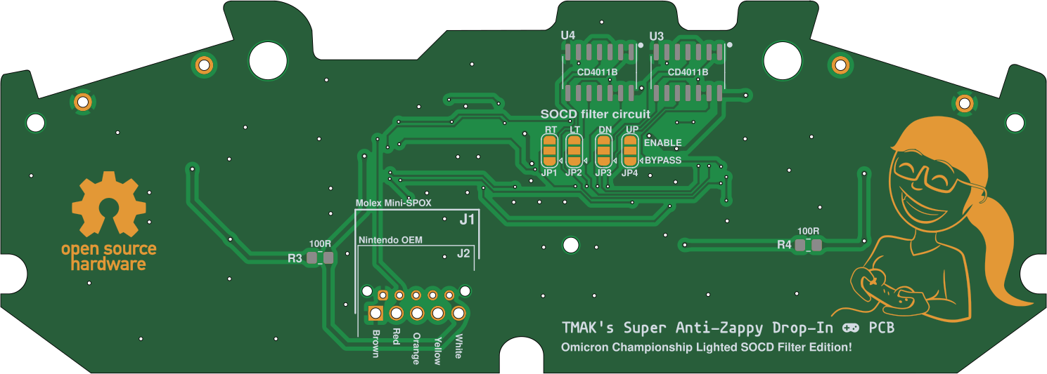
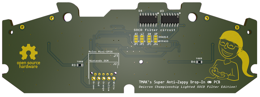
4. OPTIONAL D-Pad SOCD Filter
Applicable Board Revisions: rev_5j and newer
The SOCD filter circuit is an optional feature that uses CD4011B NAND logic gates to take something that's normally physically impossible and makes it also logically impossible: press LEFT/RIGHT or UP/DOWN on the D-pad at the same time. This is handy for people who want to build custom controllers with discrete buttons instead of a traditional D-pad.
Required BoM Components
Important
As indicated by the Ref column, the decoupling capacitors in this table are in addition to the ones required by the main controller circuitry in section 1.
| Ref | Mfg. Part # | Quantity | Description |
|---|---|---|---|
| U3, U4 | CD4011B |
2 | Quad 2-input NAND gates |
| C3, C4 | 885012007076 |
2 | Multilayer Ceramic Capacitors MLCC - SMD/SMT WCAP-CSGP 100V 10pF 0805 5% |
Assembly Steps
- Solder two 10pF SMD capacitors at C3 and C4 on the top side of the PCB.
-
Solder two CD4011B quad-NAND gate ICs at U3 and U4 on the bottom side of the PCB. Pin 1 is marked with a dot and a longer line on the silkscreen, and orientation very much does matter here.
IC ORIENTATION WARNING
These two chips are oriented upside-down with respect to the chips on the front side of the board. PIN 1 is the upper-right pin, marked with a on the board silkscreen.
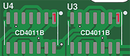
Installing these integrated circuits backward may result in permanent damage to the IC.
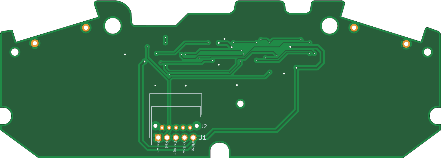
5. Wire-to-Board Header
Applicable Board Revisions: ALL
I saved this for last because it contains two options:
- Salvaged connector from a Nintendo SNES controller OR
- New Molex Mini-SPOX connector.
Which of these you use is entirely up to you, but using the original connector from a SNES controller is generally preferred because it means you don't have to re-wire a controller cable.
Option 1 (RECOMMENDED)
Applicable Board Revisions: rev_4a and newer
Salvaged Nintendo Connector
This is the best option if you have a rev_4a or newer PCB and are not building something completely custom. There is no BoM for this, just de-solder the connector from the old SNES controller and solder it in the J2 footprint on the PCB.
Option 2
Applicable Board Revisions: ALL
Be advised: special tools are required for this option. If you're using a PCB revsion older than rev_4a, this is your only option.
Required BoM Components
| Ref | Mfg. Part # | Quantity | Description |
|---|---|---|---|
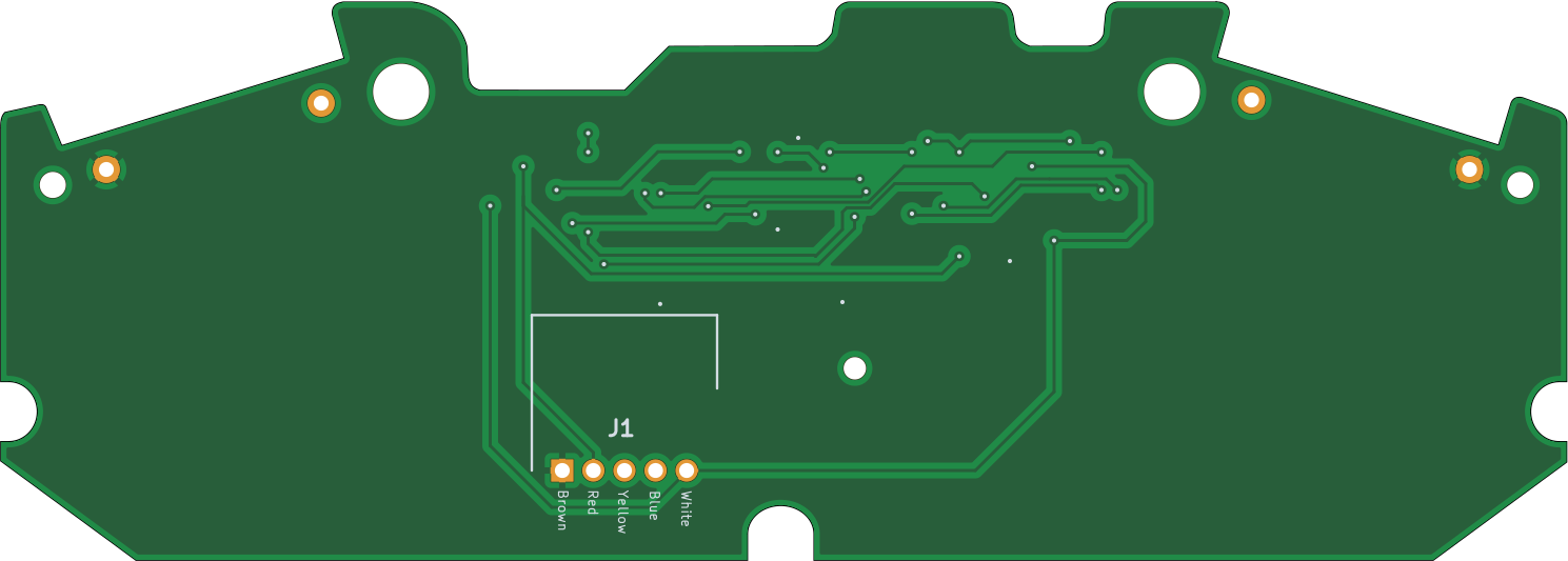
| J1 | 22-05-7055 |
1 | Molex Mini-SPOX 5-pin horizontal header |
| N/A | 50.37-5053 |
1 | Mini-SPOX 5-pin plug |
| N/A | 39-00-0160 |
5 | Mini-SPOX TERM 22-28G FEM |
Minimum Order Quantity
Most places require you to buy at least 100 of the crimp terminals for these connectors. They're usually very cheap and easy to mess up when criming, so having extras is not the worst thing in the world.
Assembly Steps
- Solder the Mini-SPOX header to the J1 footprint on the PCB.
-
Cut the old Ninendo connector off the BOARD-END of the controller cable.
Caution
I said BOARD-END! That's the end that plugs into the header on the controller PCB, NOT the end that plugs into the SNES control deck!
-
Strip about 2mm of insulation off of the wires and crimp Mini-SPOX terminals onto them.
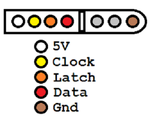
- Orient a Mini-SPOX 5-pin plug as it would plug into the header. That's wire-side facing you and bumpy-side down.
- Slot the terminals into the plug in this order (left-to-right):
- WHITE : +5V
- YELLOW : CLK
- ORANGE : LAT
- RED : DAT
- BROWN : GND
Info
If have any doubts about which wire goes where, I suggest you refer to this SNES controller pinout diagram and tone the pins out with a meter:
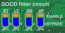
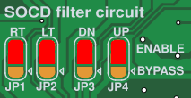
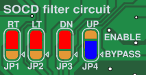
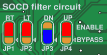
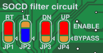
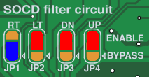
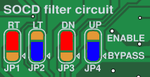
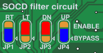
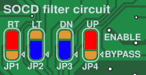
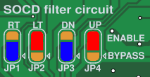
6. SOCD Filter Jumpers
Applicable Board Revisions: rev_5j and newer
On board revisions that support it, the SOCD filter circuit behavior is configurable by solder bridges between jumper pads on the back side of the PCB. If you have a board revision with these jumpers present, you must set them one way or another or the controller D-PAD will not function!
Option 1: No SOCD Filter
If you elected not to populate the SOCD filter components, then short the bottom two pads of each jumper (marked with BYPASS on the silkscreen) like so:
Option 2: SOCD Filter
This input filter circuit supports a total of nine settings combinations that can tailor - in a limited fashion - the filter behavior to your needs. Those combinations are:
This is the simplest configuration option, and the one most likely to be compatible with the widest range of game types and gameplay styles.
This style seems to be favored by tournament fighter enthusiasts.
7. Final Assembly
If you've made it this far, you should have a fully assembled board that resembles this:
Final assembly steps:
- Solder wires from each shoulder button daughter board to the tR+/tR- and tL+/tL- vias on the main controller PCB.
- Connect the controller cable to the header on the PCB.
- Reassemble your controller and test it to ensure everything is working as expected.
- I recommend using either the SNES Burn-In Test Cart or 240p Test Suite for this.
- Go play your Super Nintendo!
8. Troubleshooting
Oh no! You've finished assembling your shiny new controller board but it doesn't work right! Here are some common symptoms and possible causes.
| Symptom | Have a look at... |
|---|---|
| D-pad doesn't work at all. | Unbridged SOCD Filter jumpers. |
| Controller registers random/spazzy button inputs even when nothing is pressed. May affect some or all buttons. | Floating shift register parallel inputs due to poorly soldered resistor array(s). |
| No input at all registered from controller. | (1) Solder bridge between U2 pins 10 & 11. (2) Dry solder joints on the wire-to-board header (PCB side). (3) Loose or damaged wires/pins in the wire-to-board connector (cable side). |
| Controller doesn't work with some games (notably Donkey Kong Country series or any game that supports the SNES mouse). | (1) Are you in posession of a rev_2f board? See this post for how to bodge in a fix. (2) Solder bridge between U2 pins 7 & 8. |
| Some or all LEDs will not light up. | (1) Missing resistor at R3 and/or R4. (2) One or more LEDs installed backward. |